A Thousand Shades of Silicon
 Lately, I've been working with a lot of elemental silicon in the lab. Silicon is a pretty amazing material, both in terms of its chemistry and properties as an electronic material. Its semiconductor properties make it an essential part of this blog's existence, and thus, it serves us well to pay a brief tribute to this, the element which is primarily responsible for my pejorative and pedantic blogging.
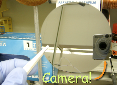
Pure silicon is beautiful stuff. Big lumps of single-crystal silicon boules have wonderful iridescent patters and reflect many different colors. Silicon wafers, after polishing, are very reflective and are usually of extreme purity: semiconductor-grade silicon, the stuff Intel and company make chips out of, is generally >99.9999% pure silicon. Silicon can be doped with other elements to enhance its semiconductor properties; for example, p-type silicon is doped with boron, and n-type silicon is doped with phosphorous. Here's a p-type silicon wafer I had lying around in the lab. Note that on the polished side, you can't even "see" the wafer itself, just the reflection. I've taken this picture Myspace-style because I am emo like that.*

Now things get a little interesting. The blue wafer on the left is silicon doped with a thin (100 nm) layer of silicon oxide (SiO2), and the wafer on the right is pure silicon. The color of the wafer is dependent on the thickness of the oxide. This makes it easy to determine the thickness of SiO2 on your substrate- just look on a color chart, like the one I just linked to. Why does the color change with the oxide thickness? I'm not well-versed in the physics, but Feynman knew a thing or two about it.
Silicon nitride, SiNx, is another crystalline silicon-based network. This plate is Si/300 nm SiO2 with some silicon nitride deposited on the surface via PECVD. The outline of the plate is purple most likely due to the lack of silicon nitride on the sides.
*I am not a photographer. Also, taking pictures of mirrors is hard.


10 comments:
Ooh, pretty!
I like the mirror shot, but I still have to kill you if you're actually emo.
some of our doped surfaces.
http://www.chemicalforums.com/index.php?topic=16336.0
I really like the word "pedantic".
Niobium has similar properties in relation to its oxide, except since it's a metal you can control the amount of oxide you form by passing a certain current through it for a certain amount of time. Varying the thickness of the oxide on the metal's surface gives it all sorts of different colors, and thus there is a bit of a movement to incorporate niobium into jewelry, both for the novelty and the varying color properties.
I know too much about this because there's a local person at one of the Durham high schools who is a semi-expert on niobium-based jewelry.
If you are growing thin films and mucking with interference, why not ding the fundamental structure of the quantum vacuum itself? Casimatter!
http://www.mazepath.com/uncleal/casimir3.htm
(Calculating Newton's G at the onset is grossly bogus. Can Dear Reader see why? The rest is mostly good chemistry, good physics, and still bogus. Could Casimatter be funded? More than likely if submitted less warnings.)
Photographing mirrors is easy. You breath on them just before making the picture, to make them foggy.
Real lab perverts pose nude in front of their mirrory scientific objects, to to get a little hairy reflection of themselves in the photo
*vomit*
No, Milkshake wins. That definitely cracked me up. (But also: ewwww.)
That's pretty cool. Right now I'm testing some silicon wafers for use in a detector my group is building. Super shiny! :D
What kind of detector? What group?
Mitch
Impressive. Maybe we should print with silicon.
Post a Comment